A world filled with teeny tiny two-dimensional electronic devices is a giant step closer thanks to a pioneering technique to make atom-thick patterns that combine a conductor and an insulator.
Conventional microelectronic devices have three basic parts; a metal to conduct electricity, semiconductor components and an insulator to protect the components from the free-flowing electricity.
“The long-term proposal is to have the different components, but all of them at the level of atomic-layer thickness,” Pulickel Ajayan, a nanomaterials scientist at Rice University, told NBC News.
He and his colleagues have successfully mated two of the three components – a conductor and insulator. The conductor is the wonder material graphene, and the insulator is hexagonal boron nitride.
Meanwhile, Tomás Palacios and his colleagues at the Massachusetts Institute of Technology are working with molybdenum disulfide to create the semiconductor piece of the puzzle.
“Ultimately, one will be able to build complete circuits with semiconductors, metals, and insulators all at the atomic level with our system,” Ajayan said.
The new technique expands earlier research that showed graphene can be merged with hexagonal boron nitride, an insulator, since they both have the same chicken-wire atomic array.
The new work, published Sunday in Nature Nanotechnology, describes a method for finely controlling the deposition of graphene onto gaps in sheets of hexagonal boron nitride through a lithorgraphic process.
“You can essentially stitch one onto the other and that enabled us to do this pretty well,” Ajayan said.
As a proof of principle, the team created designs such as combs, rings, and an owl, the Rice University mascot.

The technique starts with a sheet of hexagonal boron nitride. Then masks are laid on top the sheets. The exposed material is etched away with boron gas. Once the masks are washed away, graphene is grown in the gaps via chemical vapor deposition.
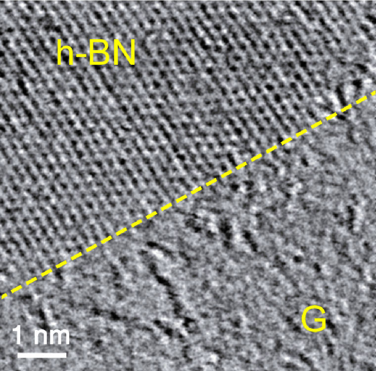
The graphene bonded with the hexagonal boron nitride, as seen in the image at left. This layer can be picked up and placed on any substrate.
Going forward, the team aims to integrate a third element, a semiconductor, to the 2-D fabric. If this works, it would allow for truly integrated in-plane devices.
“There is no limit to what you can build,” Ajayan said, who noted that functional layers could be stacked, creating a stacked devices at the atomic scale.
“You get a very robust, flexible, functional device that includes not just the device but also power and other peripherals,” he said. “That is the road we are going down.”
John Roach is a contributing writer for NBC News. To learn more about him, check out his website. For more of our Future of Technology series, watch the featured video below.
